
Malte Wagenbach
Co-Founder & CEO
Full time on Corbel. Repeat founder across energy, AI and consumer brands. Owns the plan, the money and the partners.
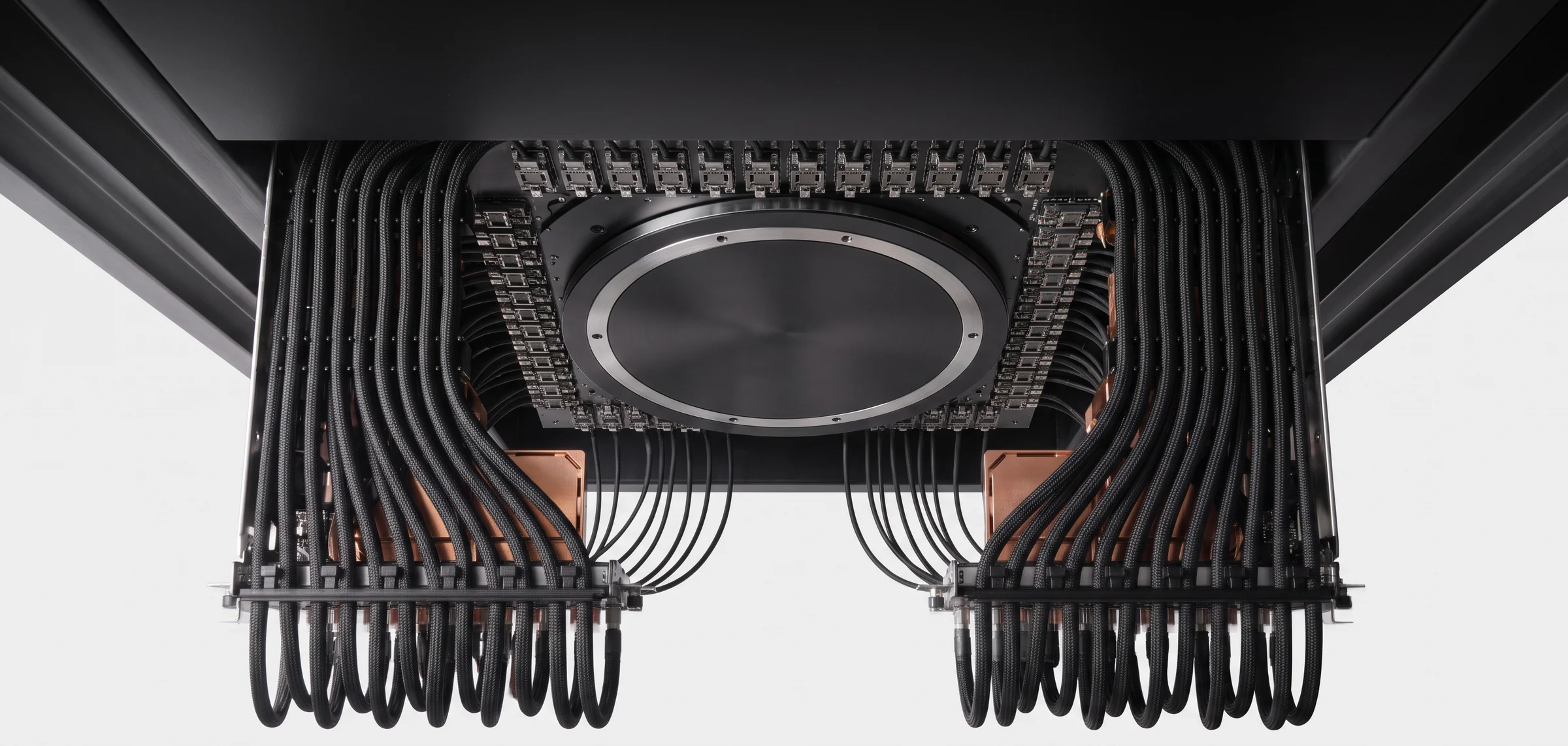
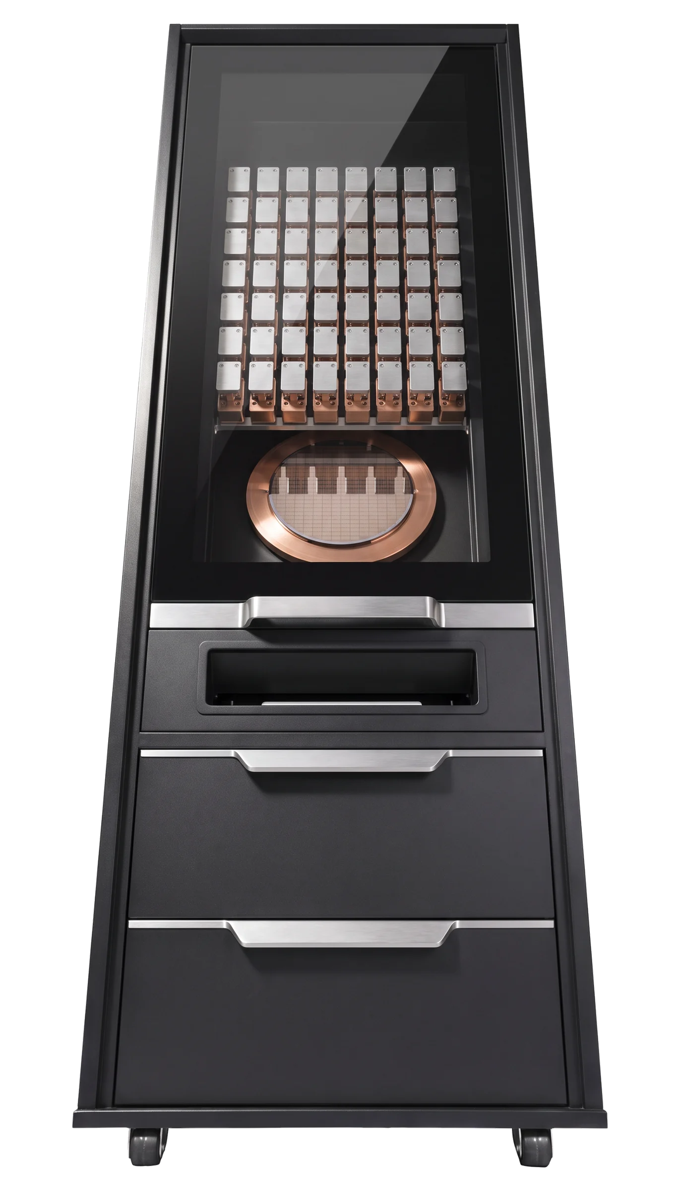
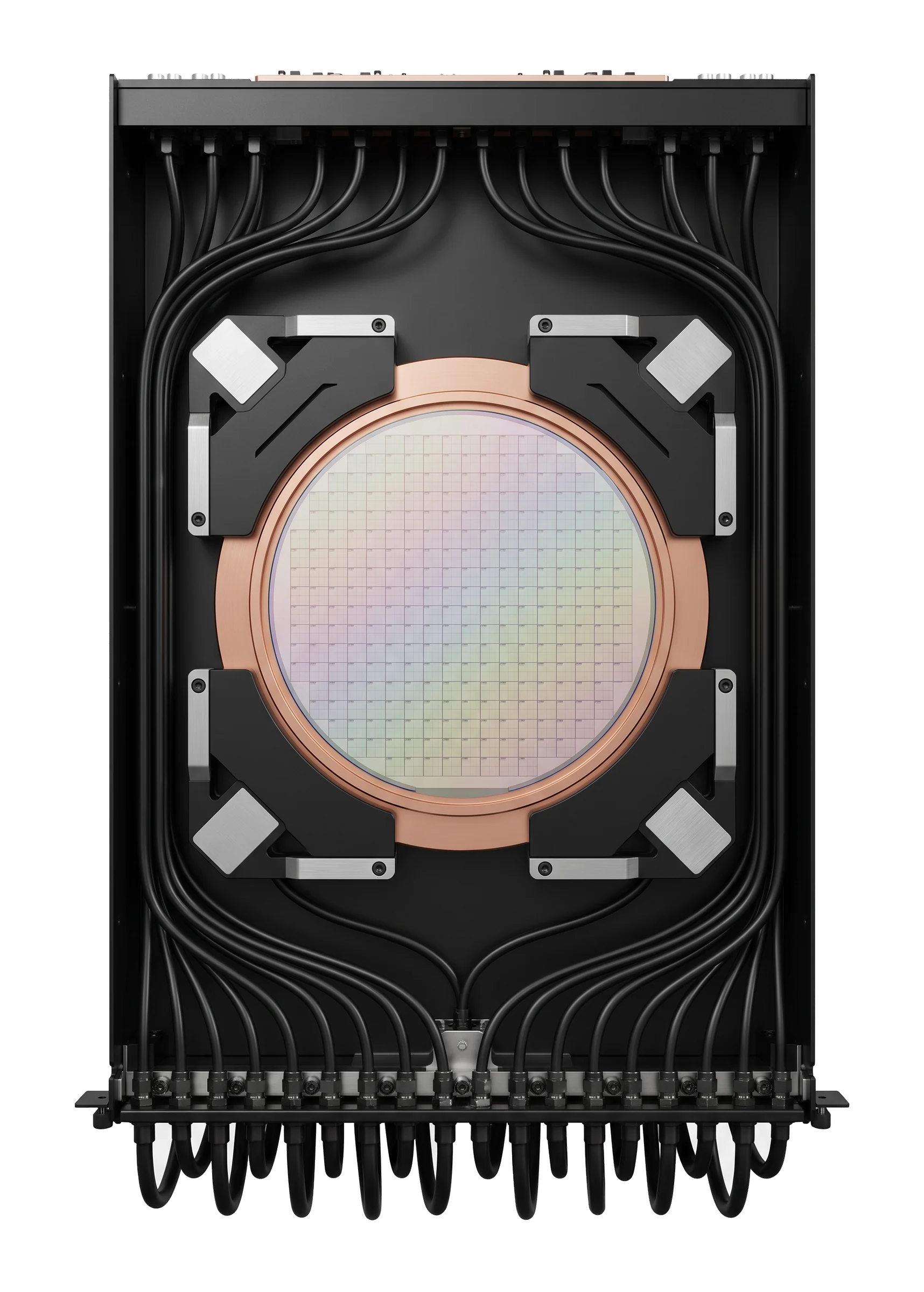
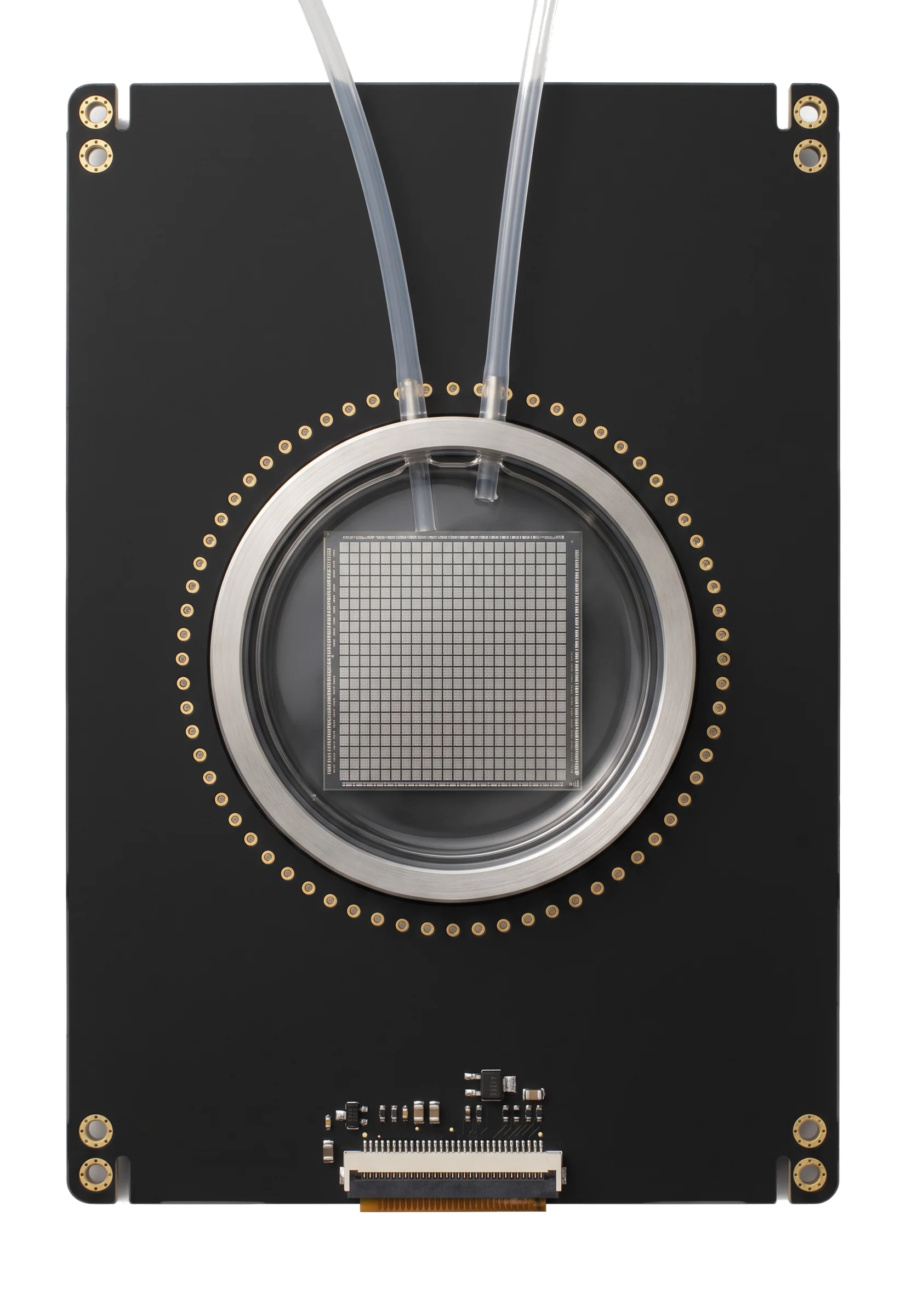
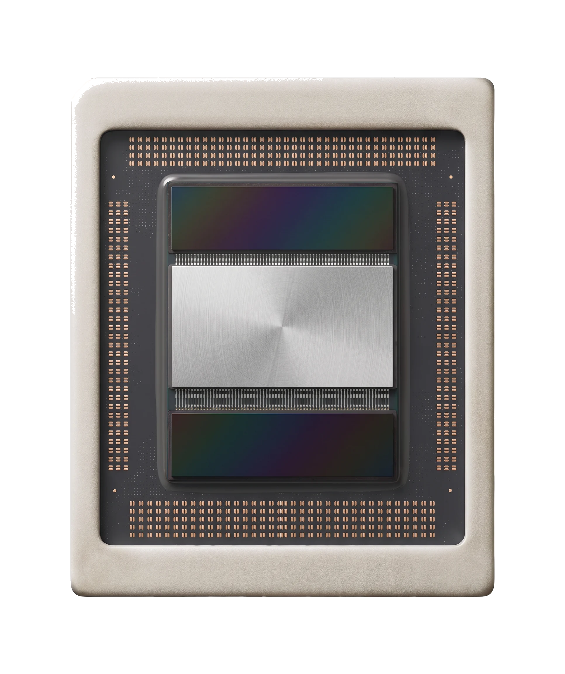
Arrays of protein nano-arms on DNA scaffolds place carbon nanotube devices at room temperature. Nothing underneath gets cooked, so logic can be built directly on top of memory instead of next to it.
Our first milestone is a dry measurement of the arms, moving and read out in dry nitrogen instead of water. That is the step between a lab result and a chip fab, and it is what our seed round pays for.
Corbel is the semiconductor spinout of the NanoDynamics Institute, the lab that built the nano-arm platform. The institute keeps developing it for every other field. We take it into chips.
A 32-bit add costs about 0.1 pJ. Reading those 32 bits from off-chip DRAM costs about 640 pJ. Most of the energy in an AI chip goes into the trip between logic and memory, not into the math. We don't make the transistor cheaper. We shorten the trip. Two ideas make that possible:
Silicon transistors need around 1,000 degrees C to form. That heat destroys the wiring below, so you can't grow logic layer by layer on top of memory. Today's stacking bonds finished dies at micron pitch. It works, but it is a coarse way up.
Our arms place carbon nanotube devices at room temperature. The layer below never sees the heat, so we can build device by device instead of die by die. Hybrid bonding stacks dies. We stack devices.
Getting there means co-designing everything from the arm to the circuit: protein and DNA design, crosslinking for stiffness, a CMOS control plane, BioFET read-out, MEMS integration, and the move from ionic solution to dry nitrogen.
One arm is slow. Ten thousand arms working side by side are not. The array grows with wafer area, so placement speed grows with it, not with time on the tool.
In soft DNA an arm runs at about 25 Hz today. The physical ceiling is near 100 kHz, and stiffer structures will run faster. We plan on a range, not a single number.
Some placements will miss. We design for that the way DRAM does: regular arrays, read-back after every step, retries, and spare rows and columns that take over from bad cells. The first product is a memory layer for exactly this reason.
The pieces are published. DNA templates have placed nanotubes (Caltech, 2010). A DNA arm has moved with nanometre precision at 25 Hz (TU Munich, 2018). A carbon nanotube processor has run code (MIT, 2019). Nobody has turned them into a manufacturing process yet. If you want to be the one who does, you should join us.
The world makes about 4 terawatts of electricity. The AI build-out wants a terawatt of chips a year. Doubling the grid in four years is not a plan. Getting far more compute out of every watt is, and the missing piece is nanoassembly that scales.
We start on the foundry's wafer. Our first product is a 3D memory layer added to a finished logic wafer in our own facility. The foundry keeps its process and its customer. No EUV in our step.
Each year the assembly cell takes on more of the stack. Protein designers sit next to process engineers, and the wet lab sits next to the clean room.
Co-Founder & CEO
Full time on Corbel. Repeat founder across energy, AI and consumer brands. Owns the plan, the money and the partners.
Scientific Founder
Physical chemist, PhD Northwestern. Over 20 years in nanofabrication, plasmonics and atomically precise manufacturing. Builds computer-controlled nanorobotics.
Head of Process
First hire from the seed round. Leads the move from wet lab to dry, fab-ready assembly. Process background in MEMS or advanced packaging.